
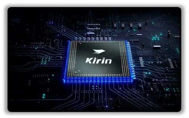
💥 Huawei claims new chip architecture will match 1.4nm process by 2031
Huawei Technologies announced plans to bring its semiconductor development capabilities to the level of a 1.4-nanometer technology node.
At the core is a key technology - the LogicFolding architecture, which reduces capacitive load on signal propagation, increasing transistor density.
Huawei's new principle, called the Tau (τ) scaling law, proposes replacing traditional geometric transistor size reduction with what the company calls "temporal scaling."
Whether LogicFolding can deliver performance up to 2nm without extreme ultraviolet lithography equipment, which is unavailable to China, remains an open question.
LogicFolding: 381 chip models released in 6 years) ⁉️
🔥 Analysis in microelectronics here
🫥 UNSERO: Digital Horizon
Comments
0No comments yet.
Sign in to join the discussion.